


Steady-State ThermoReflectance Fiberoptics (SSTR-F) combines the technological power of laser based thermoreflectance experiments with the proven measurement capabilities of steady state thermal measurements that can accommodate sample sizes as small as a few hundred microns.
Best For Liquids, and Pastes
80K – 600K
Temperature
Range
Up To 100 Microns
Spot Size
Features
SSTR-F
- Absolute measurement of thermal conductivity
- Thin films and coatings (> 1 micron)
- Effective boundary resistance (thickness <1 micron)
- Auto-scanning for thermal conductivity mapping
- No inputs (i.e. heat capacity)
FDTR
- Multi-Thermophysical Properties
- Thin films and coatings (> 5 nm)
- Thermal Boundary Resistances
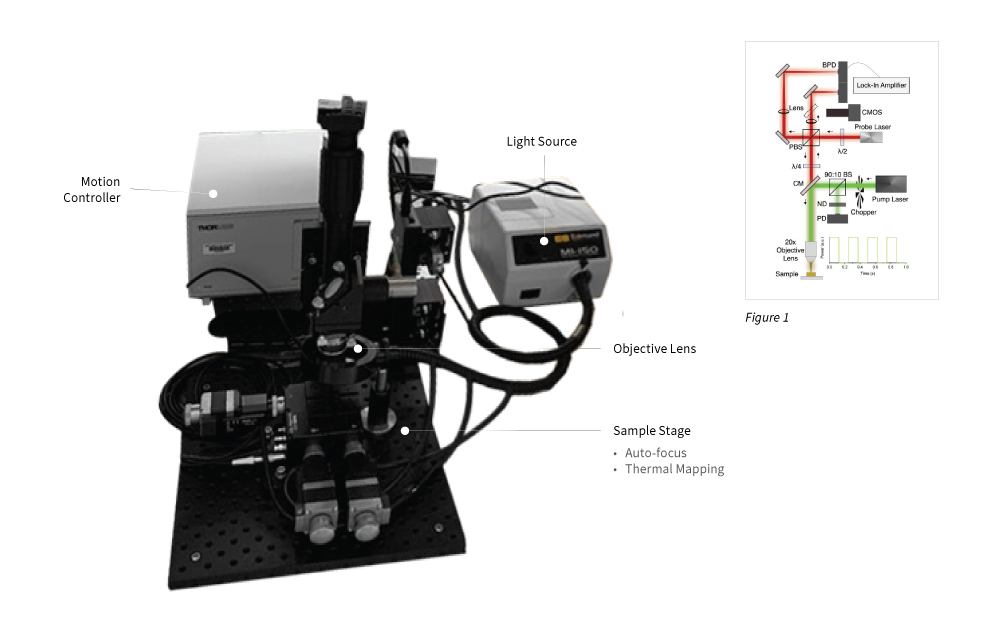
Unlike most traditional free-space (exposed laser beams) pump-probe experiments, SSTR-F incorporates all of its active and passive components in fiber-optic leading to a compact, simple system with increased safety, no need for prior optical experience, and
streamlined high throughput measurements.
The technique works in principle by inducing a steady-state temperature rise in a material via long enough exposure to heating from a pump laser. A probe beam is then used to detect the resulting change in reflectance, which is proportional to the change in temperature at the sample surface. Increasing the power of the pump beam to induce larger temperature rises, Fourier’s law is used to determine the thermal conductivity.
For expanded capabilities, the FDTR Testing Module may be added to the basic SSTR system. A key upgrade is the ability to measure thermal conductance and heat capacity of ultra-thin films – coatings down to a few nanometers thick. Understanding of the intrinsic and interface resistances between layers on a nano-scale, is a valued measurement for investigating the heat transfer efficiency of micro-electronics and related fields.
Specification
SSTR-F Specification
| Materials | Solids and Liquids |
| Thermal Conductivity Range | 0.05 to 2500 W/m•K |
| Directional Measurement | Through-thickness and In-plane |
| Spot Size | Up to 100 microns |
| Temperature Range | 80K – 600K |
| Accuracy | 5% |
| Repeatability | 2% |
FDTR Specification
| Thermal Conductivity Range | 0.05 to 2500 W/m•K |
| Directional Measurement | Through-thickness and In-plane |
| Thin-film Thickness | > 5 nm |
Sample Measurements
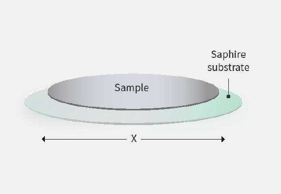
The Sample
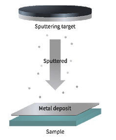
Samples of interest and sapphire sample are coated with a thin metal layer and sapphire sample is tested to determine the gamma coefficient.
Approximate Time: 1 minute
Place Sample
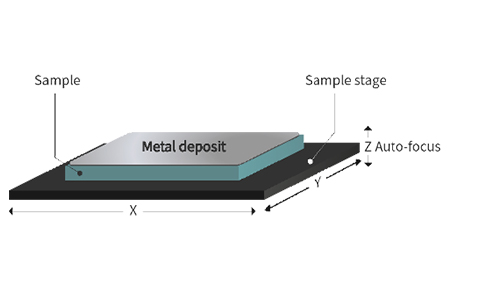
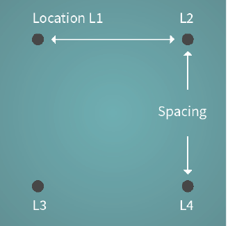
Place sample on stage, specify number of tests, and specify spacing. Based on Z direction, the sample stage auto-focuses the laser.
Approximate Time: 1 minute
Run Experiment
The scan routine starts with autofocus at every point and runs user specified number of tests.
Approximate Time: < 2 minute
Exporting Results
Calculations of thermal conductivity with associated error are computed and reported.
Approximate Time: 1 minute
Applications
Bulk High Thermal Conductivity Small Samples
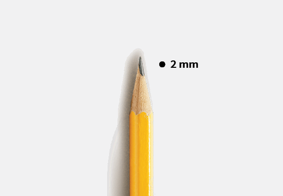
Single Crystal silicon carbide (4H-SiC) wafer pieces of 2 mm diameter x 0.5 mm thickness were measured for thermal conductivity. SSTR-F testing results of 335 W/m·K +/- 28 W/m·K, correlated well with literature values (364 W/m·K) and traditional Time-domain Thermoreflectance (TDTR) measurements of 324 W/m·K.
High Thermal Conductivity Coatings
High-purity aluminum nitride (AIN) coatings were grown on sapphire wafers at thickness of 6 μm. This coating was measured with test spot of 20 μm and 40 μm, and values were within +/- 5% of each other. The measured AIN in-plane thermal conductivity was measured at average of 283.7 W/m·K across multiple sample locations. Thermal conductivity values were observed to vary widely (+/- 36.3 W/m·K) due to micro-structure, grain size and defect concentrations. Additional measurement of bulk thermal conductivity on coatings as thin as 1 μm are also possible with SSTR-F.
High Resolution Thermal Mapping
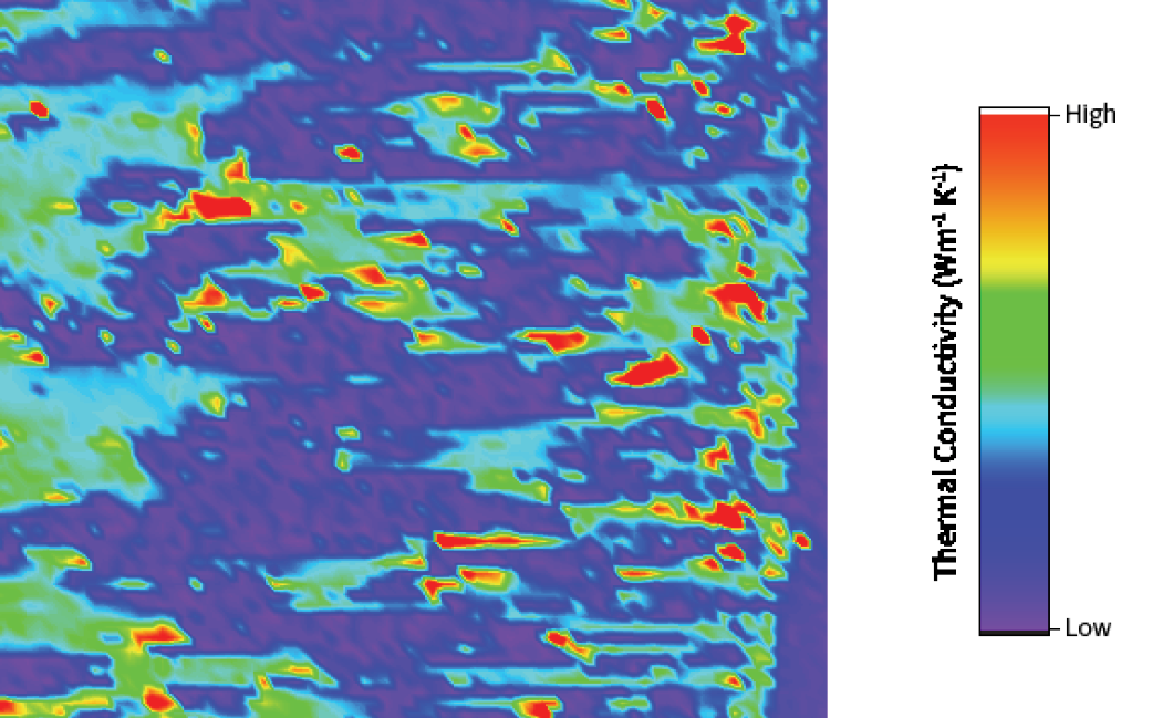
Using the SSTR-F and automated X-Y movement testing stage, users are able to thermally map their samples for thermal conductivity. The testing spot size can be changed via varying objectives from 1 to 100 microns for sensitivity tuning, while the step size can be optimized to match the micro-structural length scales of a sample.


